SC/MP: A new HEXIO card for the NDR Klein computer
Introduction
There were quite a few microcomputers in the late 70s and early 80s with seven segment displays and a hex keypad. While some used the Intel 8279 display and keypad controller, most controlled both multiplexed LEDs and a matrix keypad by software, like the standard HEXIO card of the NDR Klein Computer (NKC). That had amoung others the disadvantage of needing a timer and a timer interrupt to refresh the display or not allowing any display while the CPU was busy. The Elektor SC/MP system was a notable exception, because it performed both the LED multiplexing and the keypad button decoding (except debouncing) in hardware using TTL ICs.
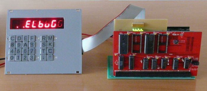
Adapting this to the NDR Klein Computer (NKC) for running the hex monitor Elbug requires a few changes. First, having one card with a bus connector was mechanically awful back then and still is, so the circuit is divided into a bus interface card connected to the display and keypad PCB by a small flat cable. Then the halt flipflop can't be used with the NKC, but fortunately it was rarely used by Elbug software and can be omitted. The reset button can't be used either, but the CPU card already offers a reset button. The result is a CPU independent HEXIO-ELEK board.
Theory of operation
The display controller uses a continuously clocked binary counter to generate a 3 bit LED address. That address is fed to a 3 to 8 decoder driving 8 PNP transistors as high side switches to sequentially enable each common anode of the seven segment displays numbered 0–7 from right to left.
The 3 bit LED address usually further passes a multiplexer to drive the 8x8 bit segment RAM, originally implemented using the half of two 7489 16x4 register files. Each data output drives a low side switch to sink the LED segment current.
Only during write accesses the multiplexer switches to pass the lower address bits to the segment RAM. That means during the write access the wrong data appears on the displays, but write accesses are too short to notice that.
Although the display RAM cannot be read back, separate IO addresses for both display and keyboard were used: 0x0–0x07 for the displays (right to left) and 0x08–0x0f for the keypad (all the same due to incomplete decoding).
The display segments a–g are assigned to the bits 0–6 and the decimal point is bit 7.
The keys are decoded using priority encoders and combined into one byte of hardware decoded bit groups for the hex keys and the command keys. Debouncing must be done in software. The bit groups are:
| 7 | 0: no key is pressed 1: key is pressed |
| 4–6 | 000: Up 001: Down 010: C 011: T 100: K 101: S 110: M 111: R or no key pressed |
| 0–3 | Value of hex key or 0000 if no key is pressed |
Details
Given the age of the design, many parts are no longer manufactured. 7489 TTL register files and their successors are all obsolete:
74 89 (16x4)
74 170 (4x4)
74 172 (4x4)
74 [23][01]x
74 189 (16x4)
74 219
74 289
74 410 (16x4)
74 870 (16x4)
74 871 (14x4)
74 910
74 989
Only the 74HCT670 is still manufactured, but with 4x4 bits it would need 4 chips. The obsolete 74LS189 can still be best obtained as new old stock, so that it is used.
The RAM has inverted outputs, so it is loaded with inverted data. If the original bit for a segment is high, it is inverted to low, the RAM outputs it inverted as high and that enables the driver switching to ground and allowing current to flow over the LED segment of the display which anode is currently powered.
Originally HP-7750 were used: Common anode, left hand decimal, 20x12.5 mm package, 25 mA avg, 150 mA peak, 1.6 V forward voltage.
Displays with common anode are common, but left hand decimal is quite rare, so a right hand decimal is used instead. A later revision of the HEXIO board used a FND507 with a right hand decimal, too. The Kingbright SA52-11SRWA has a common anode, 17.5x12.4 mm package, 20 mA avg, 155 mA peak, 1.85 V forward voltage.
On the current path, the BC177 causes around 0.2 V collector-emitter saturation voltage and the 7416 drivers need another 1.6 V, leaving 3.2 V for the LED and its series resistor, resulting in 20 mA peak current. If all segments are switched on, that is 160 mA current, which is still below the maximum current of 200 mA of the BC 177, but only due to the low side drivers.
A transistor array instead of 8 transistors and 16 resistors saves much space. The ULN2981 is rated at 500 mA per transistor (at 15 V recommended 350 mA, no spec for 5 V), which offers enough room for more current. Only one channel is used at a time. It also needs much less current to drive it, but its collector-emitter saturation voltage is 1.6 V. Replacement parts for the ULN 2981 are UDN 2981, TD62783AP and UTC 62783.
The two 7416 open collector inverters can be replaced with one ULN2803, which can sink 500 mA in total leading to at most 62.5 mA per segment. Its collector-emitter saturation voltage is around 0.9 V.
In total, 2.5 V are left for the LEDs and their resistor which results in 8 mA peak current for the LEDs. Surprisingly, that is quite bright.
The oscillator is built from a NAND Schmitt trigger with originally 330 Ohm and 100 nF, which results in a surprisingly high multiplexing frequency:
Standard TTL: f=1.2/(R*C) = 1.2/(330*100/1000000000) = 36 kHz
HCT:f=1/(K*R*C) with K=0.9 for 5.0 V supply = 33.7 kHz
Actually measured with HCT: 43.5 kHz
Unfortunately, the original design shows some ghosting and using the transistor arrays shows even more, because the high side drivers do not turn off fast enough (measured 10 us). Reducing the multiplexing frequency reduces ghosting by decreasing the ratio of glowing time to off time. Using a HCT oscillator with 10 kOhm results in 1.6 kHz (measured).
The keypad encoding has an ambiguity: Pressing a data key disables the command keys, which causes their value to be binary 111, which means the data key 0 cannot be distinguished from the command key R. That is no problem for Elbug, which always knows if it expects a command or data key, but annoying otherwise.
The data key connections are mirrored compared to the command keys, effectively inverting their bits, because the NAND gates invert them a second time.
Schematics
Mechanical design
The original keys are of high quality, but also very expensive, in particular when using labelled keycaps, and they become increasingly hard to obtain. Instead inexpensive 8x8 mm buttons are used. There are no labelled keycaps for those, but these can be 3D printed.
The total height of the key caps works out nicely to have them flush with a 19" front plate, to which the PCB is mounted with screws and standoffs. The displays are recessed, which leaves room for a red filter. The 100 uF capacitor must be mounted horizontally. All mechanical parts were designed with OpenSCAD. Experience has shown that the front plate should be manufactured in metal instead of being 3D printed for stability.
Possible improvements: Leave a little more space at the left to keep some distance between the screws and the keys, recess the connector at the right inwards or possibly solder it on the back of the board for better cable management.
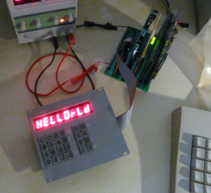
This is a NKC with ROA64, HEXIO-ELEK, IOE, CPUSCMP and BANKBOOT running Elbug:

Download
This ZIP file contains all kicad files, datasheets and 3D print designs:
hexio-elek.zip
