SC/MP: CPU card for the NDR Klein computer
Introduction
A new SC/MP system in the 21st century is really late, but I always wanted
one for personal reasons. Finally!
The
![]() NDR Klein computer
is a great modular system and the perfect
environment to bring up older CPUs with a minimal amount of work.
There is still an active group of enthusiasts that manufactures PCBs
and develops new hardware and software for it.
NDR Klein computer
is a great modular system and the perfect
environment to bring up older CPUs with a minimal amount of work.
There is still an active group of enthusiasts that manufactures PCBs
and develops new hardware and software for it.
Since hardware is nothing without software, let's have a look at the most popular SC/MP system ever: The Elektor SC/MP microcomputer. While the small MK14 single board computer, a clone of the National Semiconductor development kit with calculator keypad and seven segment display, was popular as well, it was quite limited. The Elektor system grew in a rather cluttered way to a full system with serial console and BASIC.
Its beginning was the RAMIO board (classic front panel working as DMA busmaster, RAM and GPIO with LEDs) together with a freely wired breakout board for the CPU. The address map was:
| 0000-00ff | RAM |
| 0100-01ff | 8 bit LED (incompletely decoded) |
| 0200-02ff | 8 bit input switch (incompletely decoded) |
The later system using euro cards did not use either and contained the cards CPU (CPU, driver, RAM, ROM), interrupt/multiplexer (interrupt encoder, RAM, ROM), HEXIO (7 segment LEDs with discrete controller and hex keypad) as well as additional RAM cards. Two serial interfaces for a terminal and a cassette interface were directly connected to the CPU. With time there was a switch from SC/MP to SC/MP II, which is software compatible, but not entirely pin compatible. It needs twice as many clock cycles for a micro cycle, but could run at four times the clock speed.
The interrupt/multiplexer card needs 16 ports and was incompletely decoded, but the software never used it. Its most use was to also contain some RAM and ROM.
HEXIO needs a port for the keyboard (read) and 8 ports for the LEDs (write). Both were incompletely decoded, but software never made use of that and always used the lowest addresses, so the hardware could also decode them completely. HEXIO has a discrete display controller, relieving the CPU from having to multiplex LEDs, and also decodes the keypad, leaving only debouncing to the CPU. It was used with the monitor program Elbug.
NIBL was a tiny BASIC interpreter from the manufacturer National Semiconductor, which was released to run at address 0. The Elektor system already used that for Elbug, so Elektor modified NIBL to run at address 1000 hex and called that NIBL-E. The BASIC interpreter only used the serial console interface and no further IO.
That yields the final address map of the modular system:
| 0000-05ff | Elbug ROM |
| 0600-06ff | Interrupt Encoder / Multiplexer (unused) |
| 0700-07ff | HEXIO (0700-0707 display, 0708 keyboard) |
| 0800-0bff | unused |
| 0c00-0fff | RAM (Elbug uses 0fc9-0fff) |
| 1000-1fff | NIBL-E ROM |
| 2000-???? | RAM |
After the Elektor article series in 1980 the system was maintained further in the German book "SC/MP Microcomputer Handbuch", which replaced the serial console with a CRT card and a parallel ASCII keyboard interface along with a bunch other cards. I did not find any system of that kind at the web, probably because other CPUs pushed out the SC/MP from the market.
Reconstructing the Elektor system would be much work, but building a compatible system with just a single CPU card for the modular NDR Klein computer (NKC) is rather simple.
The CPUSCMP board
This CPU board is built around the SC/MP II CPU in a way that allows to run old software. Since the NKC bus origins in the Z80 world, it features separate memory and IO address spaces. By using a comparator for the upper address byte, the IO devices can be mapped to either run NIBL or Elbug/NIBL-E. The few programs for the RAMIO can be modified using a different address for the existing NKC board IOE.
Clock
The Elektor system used a crystal with RC combination connected to the CPU. The SC/MP II ran at 2 MHz for the original CPU card and at 4 MHz for the later one, because the memory used originally did not allow more. For compatibility, being able to switch between both speeds is desirable.
The CPU can also be clocked externally using XIN. The clock is symmetrically with a phase of at least 120 ns, although the data sheet shows an asymmetric clock. By dividing the clock, a jumper allows to select between full and half speed.
Reset
The Elektor system used a power on reset on the CPU board, but could be reset from the bus as well, which was used for a reset button on the HEXIO board. The NKC always drives the reset signal on the bus from the CPU board, which has power on reset and its own reset button as well as a jumper for an external button. The TLC7705 implements all that in a reliable fashion.
As described in the datasheet, the SC/MP takes quite some time to get out of reset:
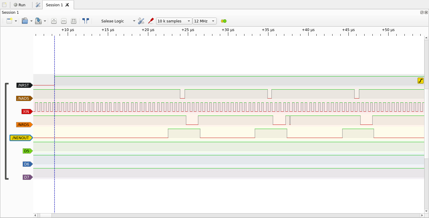
Multiplexing of data and address bus
While /NADS is active, the CPU puts the address bits A12–A15 on D0-D3, which need to be latched at the falling edge until the rising edge. One way is an inverter and a half 74 573 latch.
An easier way is a 74 395 loadable shift register, which does not need an inverter and takes less space, because it is only 4 bit wide. Its primary function as shift register is not used.
Bus cycle
The IO access signal /IORQ is used through an address area of 256 bytes, which means the addresses must be decoded before /NRDS and /NWDS. That is done using the signal ADDRVALID, which signals a valid address on the bus. It begins with the rising edge of /NBREQ to enable the comparator that selects between memory and IO access.

The generated signals /NKC_IORQ and /NKC_MREQ are active before /NKC_RD and /NKC_WR, like for the CPU68008 board, which also uses memory mapped IO, but different to the CPUZ80 which creates both signals synchronously.
The bus cycle can be extended using /NKC_WAIT connected to /NHOLD (untested).
DMA
Besides fast io transfers, DMA is a convenient way to access the memory in a new system that has no firmware yet. Back then, front panels were popular. Today an Arduino is way more convenient.
The SC/MP offers bus arbitration for symmetric multi processing: /NBREQ is the bus request signal (open collector) and /NENIN with /NENOUT is the priority daisy chain. Changes to the daisy chain are always accepted immediately and a running bus cycle is aborted and restarted later. A DMA controller acts as bus master like CPUs do. That is quite advanced, but typical peripheral controllers are not built for aborted bus cycles, so is made sure that started bus cycles are always finished before accepting a bus request using /NKC_BUSRQ by waiting until the address bus is no longer used. The bus release is then signaled using /NKC_BUSAK. There is no DMA daisy chain on the NKC.
Bus request when idle:

The bus request right before /NADS shows the CPU does not abort the cycle immediately at this point, as described in the data sheet, but still fast enough:

Slightly earlier, it does abort the cycle immediately, though:
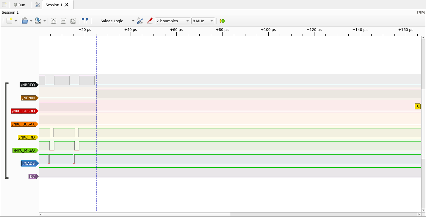
Once the cycle begins, the bus is granted after the cycle finishes:

HALT
The SC/MP HALT instruction has an uncommon meaning: It only sets a buit in the status register, which is output during multiplexing the upper address bits. If it is desired to halt the CPU, external hardware has to accomplish that by disabling CONT. That forbids to handle interrupts without further hardware. Apart from that, any other semantics could be implemented using hardware, kind of like a CPU extension. Since the semantic is not portable, HALT is rarely, if ever used by existing software and the CPUSCMP board does not use it.
UARTs
Starting with the very first development kit from National Semiconductor, all systems implemented a half duplex software UART using FLAG-0/SENSE-B, which was used as console. FLAG-0 is inverted to allow a simple discrete level shifter on the NS kit and all subsequent systems followed that convention. Due to the CPU clock of 2 or 4 MHz, timing constants had to be changed for both CPU speed and baud rate. Originally 110 baud were used with 8N2.
A second half duplex software UART is implemented using SIN/SOUT.
Both UARTs use a MAX232 level shifter (ACPE for use with 100 nF) and the edge connectors have the same pinout as the SER serial interface of the NKC.
Speaker interface
The Elektor system had a transistor connected to FLAG-1, which drove a speaker. The fanout of the SC/MP is really low, which requires a Darlington transistor. The problem of that interface is that the speaker is only driven in one direction, which distorts the sound in addition to square wave signals. A push-pull with a third transistor in front avoids that, but good operating points need even more parts. In the end using a LM386 is much easier.
The input voltage is ±0.4 V using a voltage divider made for the SC/MP fanout.
The resistor of 50 kOhm in the LM386 in combination with 330 nF is a high pass with a border frequency of 9.6 Hz:
$$f_G = 1 / { 2 · π · R · C }$$
For possibly using PWM/PDM, a LC low pass with 68 µH and 1 µF limits the output to about 20 kHz with less loss than a RC combination:
$$f_G = 20 \text"kHz"$$ $$R_l = 8 \text"Ohm"$$ $$L = R_l / { 2 · π · f_G }$$ $$C = 1 / { ( 2 · π · f_G )^2 · L }$$
LED at FLAG-2
A LED can be helpful in debugging. Due to the low fanout a transistor is required to drive the LED.
The BC547 has hFE of 200 at IC, which allows to drive up to 20 mA IC using 0.1 mA IB. 0.1 mA already load the port output to VCC - 1 V. The base voltage for saturation is 0.7 V. The base series resistor is:
$${ 5.0 \text"V" - 1.0 \text"V" - 0.7 \text"V" } / 0.1 mA = 33 \text"kOhm"$$
The cut off voltage is 0.660 V, which is met by the SC/MP using 0.4 V. The LED current is limited with 1.5 kOhm, because a few mA suffice for being bright enough.
Interrupts
The interrupt is implemented using SENSE-A, but no software ever made use of it.
Schematics

Architecture details of the SC/MP
The SC/MP has a classic architecture for its time: The memory is divided into pages of 4 KB. There are four pointer registers (p0–p3), of which p0 is the program counter. Although the registers are 16 bit wide, any pointer register arithmetic including program counter increments only works inside the page range of 12 bits. Only swapping p0 with another register for a long jump can cross pages. Changing p0 allows efficient computed jumps.
There are no 16-bit operations of any kind, which makes the SC/MP endianless and loading/storing the pointer registers very slow. By convention, 16 bit data is stored big endian. All computations involve the accumulator with the exception of memory increment/decrement.
There is no dedicated stack pointer, but there is an auto increment address mode for the pointer registers allowing to use any as a stack:
 st @-1(p2)         ; push A
 ld @1(p2)          ; pop A
Note that auto indexing uses pre decrement and post increment.
Subroutine calls are done using branch-and-link by loading a pointer register and exchanging it with the PC. Nested calls need to save the pointer register containing the return address. No doubt this was influenced by the IBM/360 BALR instruction, whereas all subsequent microprocessors used the stack for CALL/RET instructions. Amusingly, omitting the memory access matches a pipelined RISC architecture better, so branch-and-link returned e.g. with ARM.
Local variables are addressed either PC-relative or through a pointer register, which points to either static working space or a stack frame. By convention, p2 is the stack/workspace/frame pointer and p3 holds the call/return address. Workspace addressing is limited to a signed byte offset. In assembler, a page typically holds multiple functions and call frames are small, which matches the architecture. Although p2 could be used as stack pointer, a stack offers very limited addressing. Using it as a workspace or frame pointer of statically allocated frames requires a slow load and restore, which can be partially optimized away by combining the frames of multiple functions. The monitor program Elbug uses combined frames (but a different and very slow way of calling functions).
Assume upon function entry p3 contains the return address, p2 points to the frame where function arguments are addressed with negative offsets, offsets 0/1 store the callee p2 and 2/3 store the caller p3 if the function contains calls. Locals are stored at positive offsets. The function would return with:
 ld 2(p2)           ; Restore p3 if this function made calls
 xpah p3
 ld 3(p2)
 xpal p3

 ld 0(p2)           ; Restore caller p2
 xae                ; E holds caller higher p2
 ld 1(p2)           ; A holds caller lower p2
 xpal p2
 lde
 xpah p2            ; caller p2 is now restored

 xppc p3            ; return
A function would be called with:
 ldi l(newframe)
 xpal p2
 xae                ; E holds lower caller p2
 ldi h(newframe)
 xpah p2            ; A holds higher caller p2
 st 0(p2)
 lde
 st 1(p2)           ; caller frame pointer is now saved in new frame

 ldi l(function-1)
 xpal p3
 ldi h(function-1)
 xpah p3

 xppc p3            ; call function
It is more efficient to use p2 as frame pointer of stack allocated frames: The stack has to fit into a single page, but then the auto increment and decrement can be used to push and pop whole frames in a single instruction. Assume the stack grows down and upon function entry, p3 contains the return address, p2 points to the frame where function arguments are address with positive offsets and the offsets -1/-2 store the caller p3 if the function contains calls. Locals and arguments of called functions are address with negative offsets. The function would return with:
 ld -2(p2)          ; Restore p3 if this subroutine made calls
 xpah p3
 ld -1(p2)
 xpal p3

 xppc p3            ; Return
A function would be called with:
 ld @-framesize(p2) ; decrease p2 to point below arguments
 ldi l(function-1)
 xpal p3
 ldi h(function-1)
 xpah p3

 xppc p3            ; call function

 ld @framesize(p2)  ; restore caller p2
If it is desired to keep the frame pointer at the end of the frame, only half of it can be addressed and the caller has to increase and decrease it, which is the same effort.
The SC/MP lacks any kind of system call instruction, software interrupt or exception, which is a serious restriction to implement breakpoints. The original SC/MP low cost development system offered a flipflop that switched the the address bus multiplexers from the CPU address bus to a clock triggered counter in order to execute breakpoint code. The SC/MP offers an interrupt that uses p3 as interrupt vector while interrupts are enabled, which is a serious obstacle on this register starved architecture.
The PC is incremented before fetching the opcode, not after decoding the instruction, which means execution starts at address 1 and branch targets are one byte before the actual address. That's why ROM boot code has a NOP as place holder at address 0.
The NOP instruction is not special, because all undefined opcodes are a NOP. Single byte opcodes like NOP take 5 microcycles, double byte opcodes (MSB set) take 10 microcycles.
Thinking about the SC/MP from a compiler writer's perspective, the stack and all memory objects must not cross page boundaries. Jumps need to be encoded either long or short and generated code only has A, E and P1 available and needs to spill pretty much any CSE into locals. The compiler needs to track page boundaries in code and generate long jumps to cross those, or must make sure functions never cross page boundaries.
So, why did the SC/MP lose against the MCS-48? NS vs. Intel? Cost? More chips for a minimal system? From a programming standpoint, both are not exactly pleasant to use and slow, but the MCS-48 has a fixed interrupt vector and a second register set, which makes working with interrupts much easier. In assembler CALL/RET and the availability of far jumps are pleasant. The SC/MP is a classic accumulator machine. It is tempting to use the pointer registers as data registers, but frustrating that the only way to access them is by swapping them with A — they were just not meant to used for data. The assembler manual contains very little information about how the SC/MP was intended to be programmed. Left on their own, some people even claimed the SC/MP has no stack pointer, which shows the architecture was not understood well. At the time, the mainframe and the micro world were very separated. The developers of the SC/MP were likely familar with mainframes as development systems, but their customers were not.
BOM
I manufactured prototypes at JLCPCB, but found two bugs (pin 1 of the TLC7705 should be connected with 100 nF to ground, not directly, pin 5 of the TLC7705 needs a 10k pullup). The provided schematics and Gerber files are fixed, but were never manufactured. The silk screen could be more helpful, because I did not export the part values. J4 and J5 are not in the order you may expect (console is right, not left).
![]() Gerber files
Gerber files
17x 100 nF ceramic 2.5 mm pitch
1x 330 nF ceramic 2.5 mm pitch
1x 1 uF/10 V electrolytic 3.5 mm pitch radial
1x 22 uF/10 V electrolytic 3.5 mm pitch radial
1x 200 uF/10 V electrolytic 3.5 mm pitch radial
1x LED green 3 mm
1x pin header angled 50p 2.54 mm pitch (Reichelt SL 1X36W 2,54)
1x pin header 2x8p straight 2.54 mm pitch
2x pin header 1x2p angled 2.54 mm pitch
2x pin header 1x5p angled 2.54 mm pitch
1x pin header 1x3p straight 2.54 mm pitch
1x 68 uH inductor radial 5.00 mm pitch
1x BC547 TO92
1x 1.5k axial 1/4 W
1x 5.6k axial 1/4 W
1x 10k axial 1/4 W
1x 22k axial 1/4 W
1x 33k axial 1/4 W
1x 82k axial 1/4 W
2x 10k array sip9 (Reichelt SIL 9-8 10K)
1x button 6 mm pitch
1x DIP40 socket
5x DIP20 socket
2x DIP16 socket
3x DIP14 socket
2x DIP8 socket
4x 74LS245 DIP
1x 74LS04 / 74HCT04 DIP
1x 74LS00 / 74HCT00 DIP
1x 74LS688 / 74HCT688 DIP
1x 74LS395 / 74HCT395 DIP
1x 74LS74 / 74HCT74 DIP
1x LM386 DIP
1x INS8060
1x MAX232 ACPE DIP
1x TL7705A DIP
1x 4 MHz crystal oscillator DIP14